

Circuit BoardS. Fast.
PCB manufacturing that moves as fast as you do.
Utilize uFab’s patent-pending technologies to help your organization rapidly deploy PCB designs in-house within 4 hours.
PCB Quick-turn like no one else
Need your boards yesterday?
Print rigid, flex, ceramics, and more, all made in-house, without a fab house.


The uFab Edge
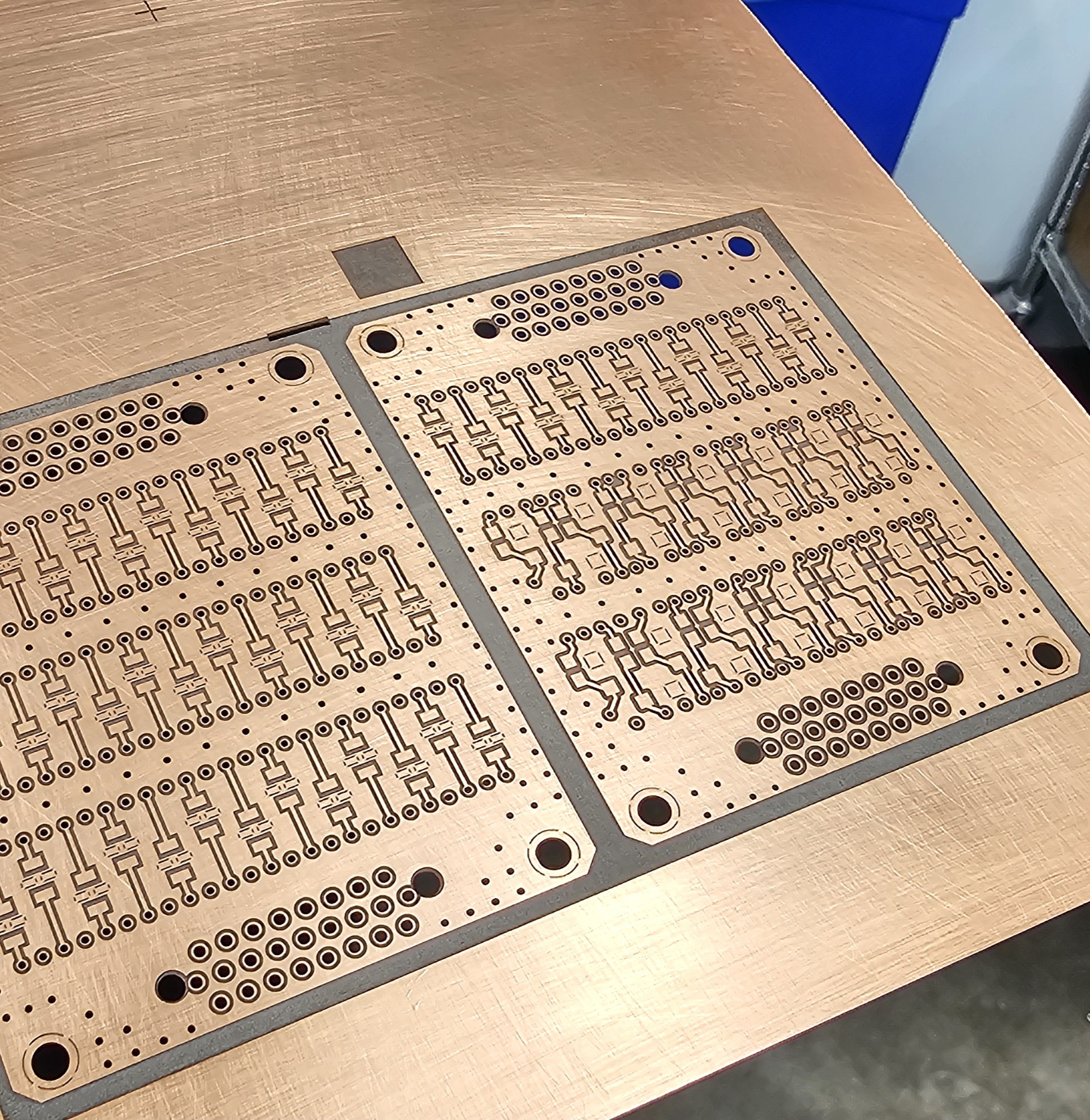
The PCBee is a laser-Based Circuit Board manufacturing machine that is ideal for in-house PCB (Printed Circuit Board) Prototyping and small batch production.
✓ Intellectual Property Security
Problem: PCB fabrication companies typically use cloud servers for managing designs and intellectual property, with many outsourcing development to overseas suppliers. This approach can expose sensitive IP to risks in global supply chains.
Solution: The PCBee operates on-site. As a standalone unit, it doesn’t require internet connectivity, ensuring secure, efficient in-house prototype production. Files do not need to be saved to your unit. This guards your IP against risks like data breaches and supply chain disruptions common in external fabrication.
✓ Zero Lead Time Prototyping
Problem: The traditional PCB fabrication process often spans four weeks for each PCB iteration. This timeline is largely due long fab house lead times, back-and-forth communication between engineers and suppliers, and more, which can stretch the development of a suitable prototype over several months.
Solution:
The PCBee rapidly produces PCBs in a matter of hours, even with exotic materials, a stark contrast to the usual weeks or months. It allows for instant in-house printing from design files. Boards made by PCBee are ready to go from the machine directly to mass production, no redesigns required. This offers a hassle-free shift from prototype to large-scale manufacturing, streamlining the entire PCB production process.
✓ Substrate Agnostic
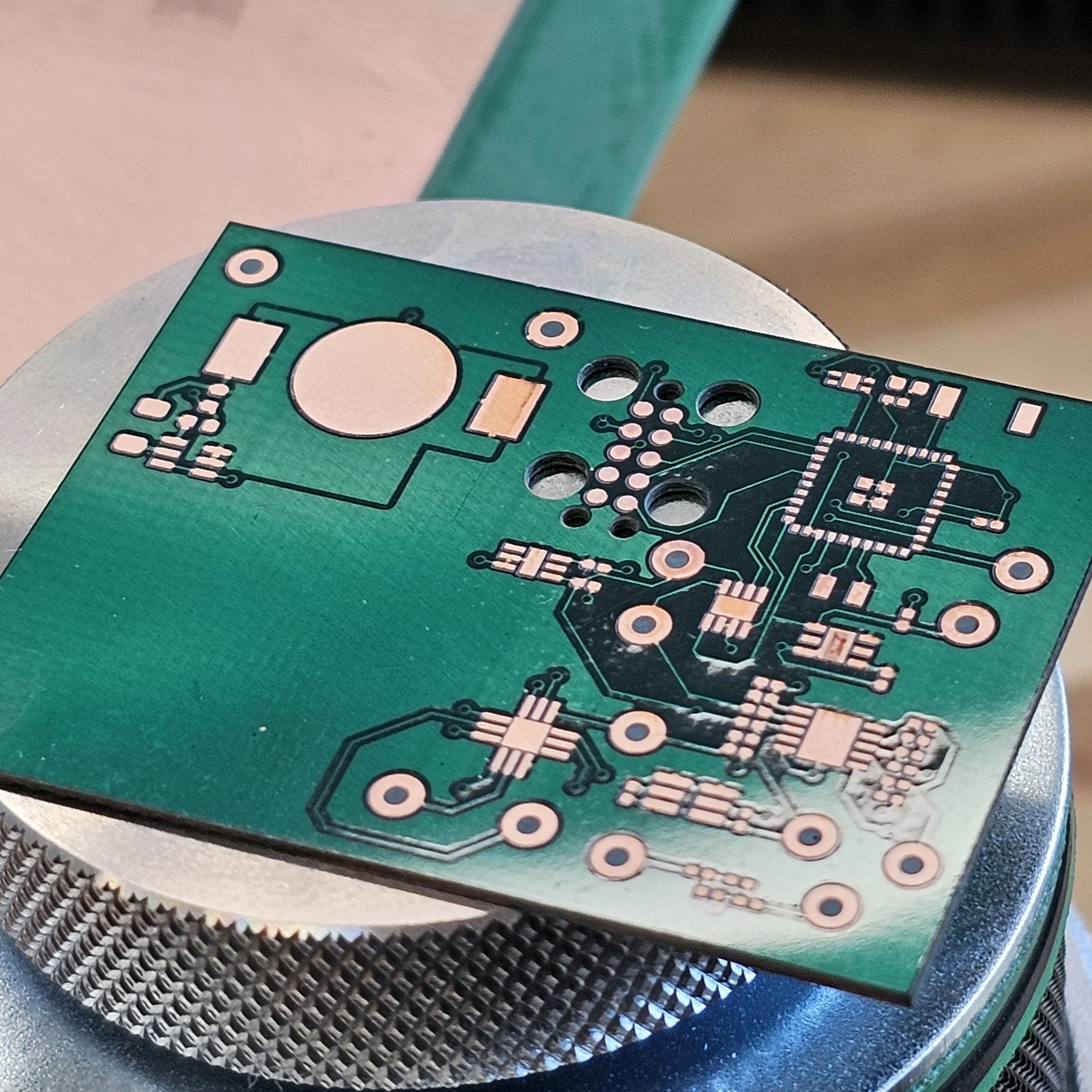
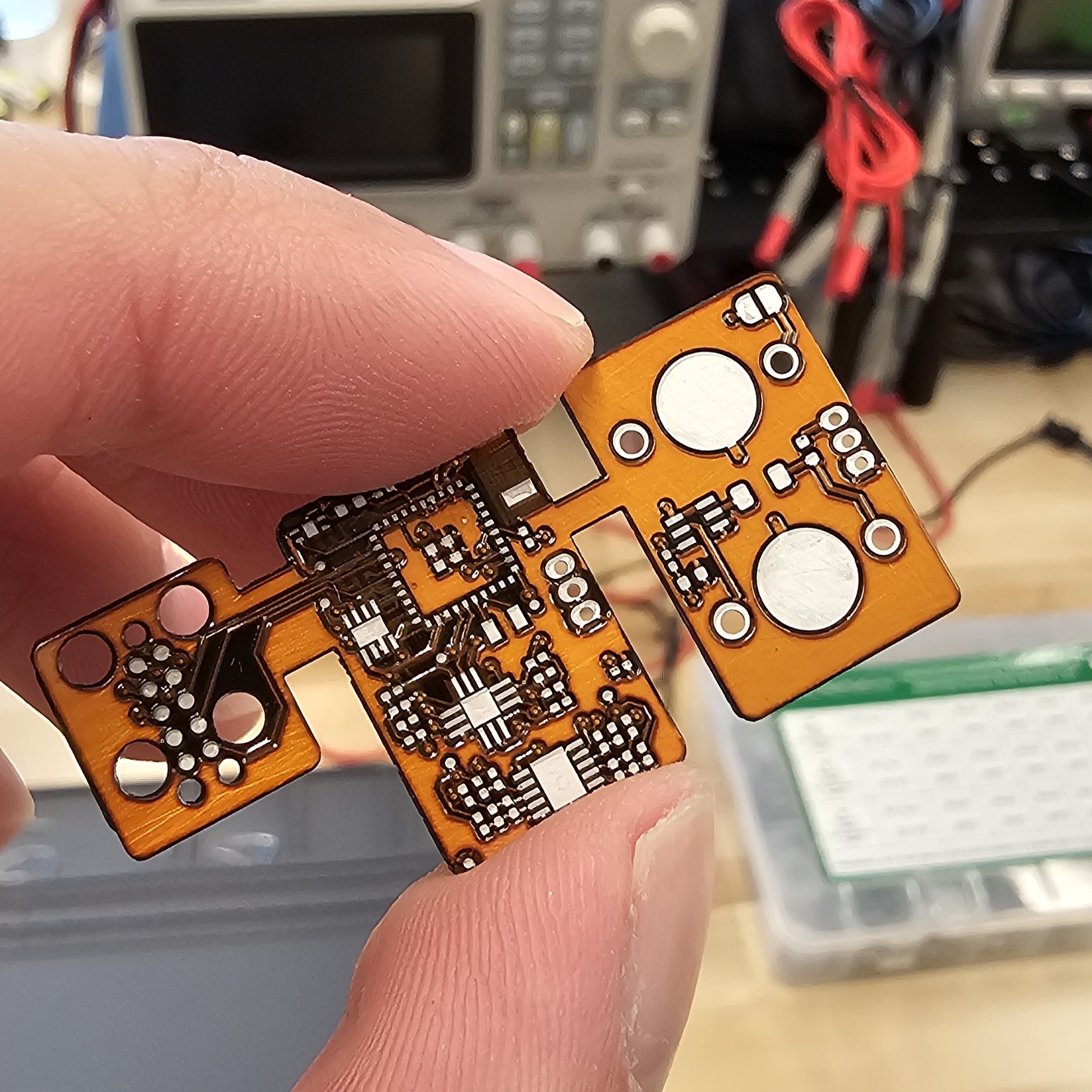
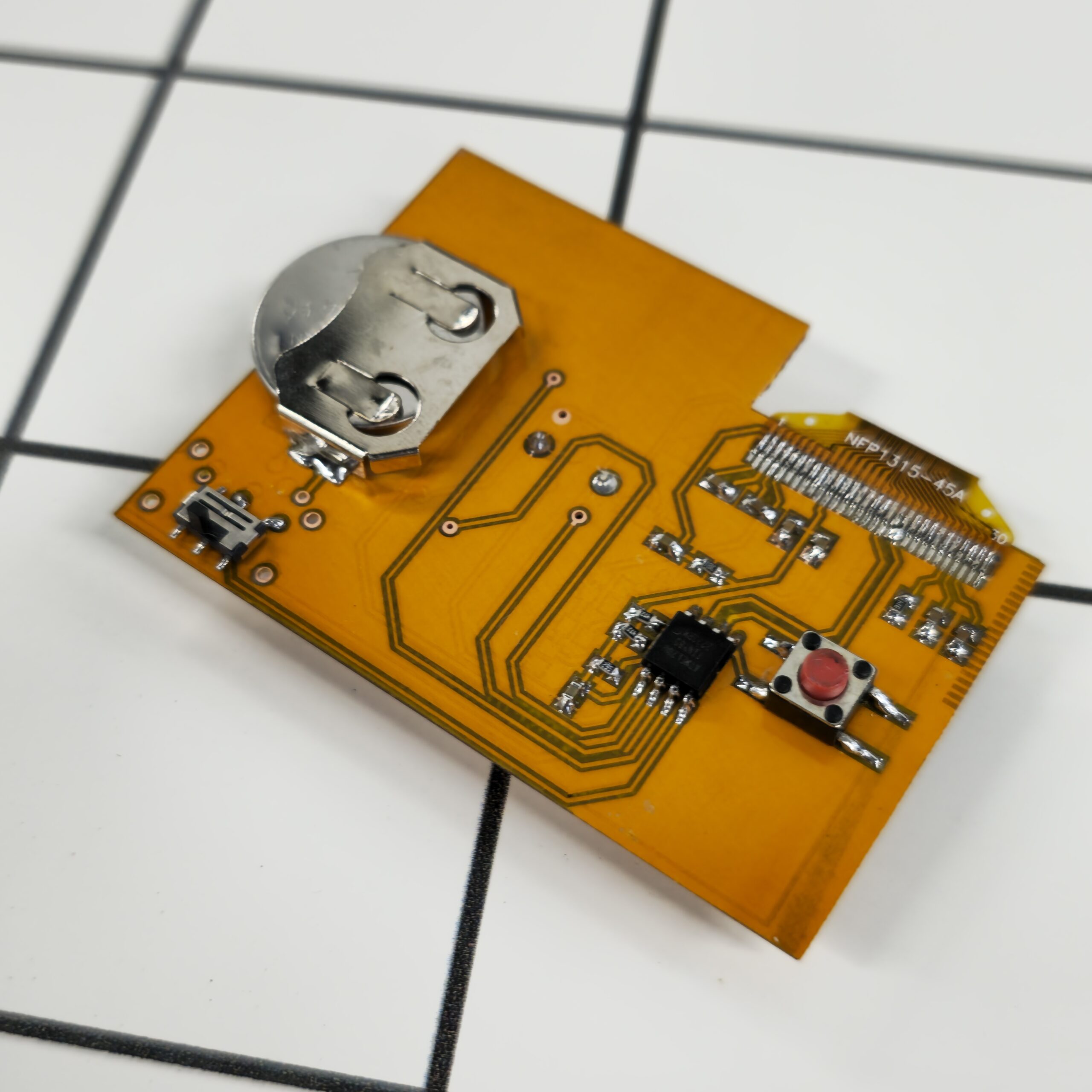
The PCBee’s design allows it to print on a variety of circuit board materials, showcasing its adaptability across different industries. It handles traditional FR4, the standard “green PCB,” used in countless applications, and offers enhanced versions for high current scenarios. Flexible PCBs, another specialty, are key in wearable tech, medical devices, and aerospace, offering the necessary flexibility for these advanced applications. Ceramic PCBs, preferred in RF applications, cater to specific needs in research, telecommunications, and RF sectors due to their superior thermal conductivity and frequency performance. Lastly, aluminum PCBs, ideal for high power and heat scenarios, are extensively used in automotive, LED, and drone industries. The PCBee’s ability to work with such a diverse range of materials is a testament to its versatility, and for those interested in exploring more exotic materials, a dedicated section on the website invites inquiries, opening a gateway to even more specialized applications.
✓ No Chemical Hazards or Toxic Waste
The PCBee stands out not only for its efficiency but also for its environmental friendliness and safety. By eliminating the need for environmentally hazardous chemicals traditionally used in PCB manufacturing, it ensures a greener production process. This aspect is especially crucial in today’s eco-conscious world, where minimizing environmental impact is a priority. Additionally, the absence of hazardous chemicals in the printing process significantly reduces liability concerns for universities, laboratories, and other institutions. They no longer have to worry about the risks associated with their employees handling, spilling, or ingesting toxic substances. This makes the PCBee a safer, more responsible choice for PCB production, aligning with the increasing emphasis on environmental responsibility and workplace safety.
The PCBee is uFab’s flagship rapid PCB manufacturing machine. In 4 hours or less, it can take a PCB from design files to physically in your hands.
Quick Inquiry
QUOTES & INQUIRIES
If you’re interested in obtaining a quote, learning more about our machine, or connecting with us, please don’t hesitate to complete the inquiry form, we will promptly get in touch with you.
Alternatively, feel free to reach our over the phone or email. We look forward to assisting you with your PCB needs and contributing to the success of your endeavors.
CONTACT US
U-FAB
911 Washington Ave,
STE 658, St. Louis MO
Copyright uFab 2026